- 您现在的位置:买卖IC网 > Sheet目录1999 > ICS951402AGLF (IDT, Integrated Device Technology Inc)IC TIMING CTRL HUB P4 48-TSSOP
20
Integrated
Circuit
Systems, Inc.
ICS951402
Advance Information
0660—05/05/05
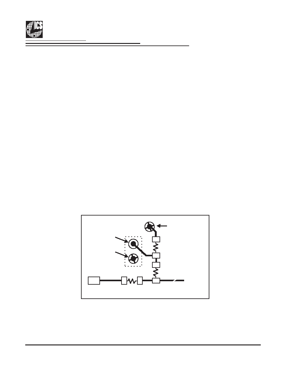
Fig. 1
Shared Pin Operation -
Input/Output Pins
The I/O pins designated by (input/output) serve as dual
signal functions to the device. During initial power-up, they
act as input pins. The logic level (voltage) that is present on
these pins at this time is read and stored into a 5-bit internal
data latch. At the end of Power-On reset, (see AC
characteristics for timing values), the device changes the
mode of operations for these pins to an output function. In
this mode the pins produce the specified buffered clocks to
external loads.
To program (load) the internal configuration register for
these pins, a resistor is connected to either the VDD (logic 1)
power supply or the GND (logic 0) voltage potential. A 10
Kilohm (10K) resistor is used to provide both the solid CMOS
programming voltage needed during the power-up
programming period and to provide an insignificant load on
the output clock during the subsequent operating period.
Via to
VDD
Clock trace to load
Series Term. Res.
Programming
Header
Via to Gnd
Device
Pad
2K
W
8.2K
W
Figure 1 shows a means of implementing this function
when a switch or 2 pin header is used. With no jumper is
installed the pin will be pulled high. With the jumper in
place the pin will be pulled low. If programmability is not
necessary, than only a single resistor is necessary. The
programming resistors should be located close to the series
termination resistor to minimize the current loop area. It is
more important to locate the series termination resistor
close to the driver than the programming resistor.
发布紧急采购,3分钟左右您将得到回复。
相关PDF资料
ICS95V847AGIT
IC CLOCK DRIVER 2.5V 24-TSSOP
ICS95V850AGT
IC CLK DVR PLL 1:10 48TSSOP
ICS95V857ALT
IC CLK DVR PLL 1:10 40TVSOP
ICS95V857CKLF8
IC CLK DVR PLL 1:10 40VFQFN
ICS97U870AKT
IC CLK DVR PLL 1:10 40VFQFN
ICS97ULP877AHT
IC CLOCK DRIVER 1.8V LP 52-BGA
ICS97ULP877BKLFT
IC CLOCK DRIVER 1.8V LP 40VFQFPN
ICS98UAE877AHLFT
IC CLOCK DRIVER 1.8V LP 52-BGA
相关代理商/技术参数
ICS951402AGLFT
功能描述:IC TIMING CTRL HUB P4 48-TSSOP RoHS:是 类别:集成电路 (IC) >> 时钟/计时 - 专用 系列:TCH™ 标准包装:28 系列:- 类型:时钟/频率发生器 PLL:是 主要目的:Intel CPU 服务器 输入:时钟 输出:LVCMOS 电路数:1 比率 - 输入:输出:3:22 差分 - 输入:输出:无/是 频率 - 最大:400MHz 电源电压:3.135 V ~ 3.465 V 工作温度:0°C ~ 85°C 安装类型:表面贴装 封装/外壳:64-TFSOP (0.240",6.10mm 宽) 供应商设备封装:64-TSSOP 包装:管件
ICS951402YFLF-T
制造商:ICS 制造商全称:ICS 功能描述:Programmable Timing Control Hub for P4 processor
ICS951402YGLF-T
制造商:ICS 制造商全称:ICS 功能描述:Programmable Timing Control Hub for P4 processor
ICS951403
制造商:ICS 制造商全称:ICS 功能描述:AMD-K7 System Clock Chip
ICS951403YFLF-T
制造商:ICS 制造商全称:ICS 功能描述:AMD-K7 System Clock Chip
ICS951403YGLF-T
制造商:ICS 制造商全称:ICS 功能描述:AMD-K7 System Clock Chip
ICS951411
制造商:ICS 制造商全称:ICS 功能描述:System Clock Chip for ATI RS400 P4TM-based Systems
ICS951411BGLF
功能描述:IC SYSTEM CLOCK CHIP P4 56-TSSOP RoHS:是 类别:集成电路 (IC) >> 时钟/计时 - 专用 系列:PCI Express® (PCIe) 标准包装:1,500 系列:- 类型:时钟缓冲器/驱动器 PLL:是 主要目的:- 输入:- 输出:- 电路数:- 比率 - 输入:输出:- 差分 - 输入:输出:- 频率 - 最大:- 电源电压:3.3V 工作温度:0°C ~ 70°C 安装类型:表面贴装 封装/外壳:28-SSOP(0.209",5.30mm 宽) 供应商设备封装:28-SSOP 包装:带卷 (TR) 其它名称:93786AFT